Advanced Tutorial
This set of tutorials focuses on explaining more advanced features that the SPiRA framework has to offer. We go into more details on how to create device and circuit PCells, how to structure a design, and how to manipulate layout elements.
In SPiRA PCells can be divided into two categorises, spira.Device and spira.Circuit.
Each of these classes contains a set of different back-end algorithms that are automatically executed when
the layout class is constructed. Typically, these algorithms consists of boolean operations and filtering algorithms.
Also, inheriting from these classes defines the purpose of the layout, either a device or a circuit.
Devices:
Similar to creating a PCell, constructing a device cell required inheriting from spira.Device
instead of spira.PCell. In superconducting circuits a device layout is usually a Via or a Junction.
class Junction(spira.Device):
    pass
Circuits:
A circuit PCell is designed similar to that of a device. By definition a circuit layout contains polygon
routes that connects different device and ports instances. Therefore, a spira.Circuit contains
two extra, but optional, create methods to simplify the code structure:
create_structures: Defines the device instances.create_routes: Defines the routing paths between different structures and ports.
class Jtl(spira.Circuit):

    def create_structures(self, elems):
        return elems

    def create_routes(self, elems):
        return elems
Note, it is not required to use these methods, but designing large circuits can cause the
create_elements method to become cumbersome.
Library Structure
Every design environment connects to a specific fabrication process, also known as the PDK.
In SPiPA, the PDK data is encapsulated in Python scripts and are collectively called the RDD.
RDD script names start with db_ as illustrated below.
This section discusses how to organize your design project in SPiRA as a systematized library. Technically, your library can have any structure given that you compensates for the necessary importing changes. But it is highly adviced to use the proposed structure.
technologies
|__ mitll
    |__ devices
        |__ junction.py
        |__ vias.py
    |__ circuits
        |__ jtl.py
        |__ dcsfq.py
    |__ db_init.py
    |__ db_process.py
    |__ db_lvs.py
The technology library is broken down into 3 parts:
- Devices: Contains defined device PCells for the specific technology.
- Circuits: Contains PCell circuits created using the specific technology.
- Database: Contains a set database files that make up the RDD.
The technologies folder is the base folder inside the SPiRA design environment that
contains all the different technology processes and PCell designs in a single place. The library structure
above contains the mitll library, which consists of defined junction and via devices, a long
with a JTL and DCSFQ circuit.
The db_init script is the first file to be executed when the RDD database is constructed.
The db_process script contains most of the information required to design a PCell.
This file contains the process layers, layer purposes, process parameters, etc.
The db_lvs script defines the created device PCells to be used in the device detection
algorithms when doing LVS extraction.
YTron
In this example we will start from the beginning. First, we will create a yTron shape and then using this shape we will create a device containing input/output ports. This device will then be used to create a full circuit layout.
Demonstrates
- How to create your own shape class.
- How to create a device and a circuit PCell.
- How to restrict a design to only accept a specific shape or device.
We create our own yTron shape by inheriting from spira.Shape, which allows us
to manipulate the shape once it has been instantiated.
class YtronShape(spira.Shape):
    """ Class for generating a yTron shape. """

    rho = NumberParameter(default=2, doc='Angle of concave bend between the arms.')
    arm_lengths = CoordParameter(default=(5,3), doc='Length or the left and right arms, respectively.')
    source_length = NumberParameter(default=5, doc='Length of the source arm.')
    arm_widths = CoordParameter(default=(2,2), doc='Width of the left and right arms, respectively.')
    theta = NumberParameter(default=10, doc='Angle of the left and right arms.')
    theta_resolution = NumberParameter(default=10, doc='Smoothness of the concave bend.')

    xc = Parameter(fdef_name='create_xc')
    yc = Parameter(fdef_name='create_yc')
    arm_x_left = Parameter(fdef_name='create_arm_x_left')
    arm_y_left = Parameter(fdef_name='create_arm_y_left')
    arm_x_right = Parameter(fdef_name='create_arm_x_right')
    arm_y_right = Parameter(fdef_name='create_arm_y_right')
    rad_theta = Parameter(fdef_name='create_rad_theta')
    ml = Parameter(fdef_name='create_midpoint_left')
    mr = Parameter(fdef_name='create_midpoint_right')
    ms = Parameter(fdef_name='create_midpoint_source')

    def create_rad_theta(self):
        return self.theta * np.pi/180

    def create_xc(self):
        return self.rho * np.cos(self.rad_theta)

    def create_yc(self):
        return self.rho * np.sin(self.rad_theta)

    def create_arm_x_left(self):
        return self.arm_lengths[0] * np.sin(self.rad_theta)

    def create_arm_y_left(self):
        return self.arm_lengths[0] * np.cos(self.rad_theta)

    def create_arm_x_right(self):
        return self.arm_lengths[1] * np.sin(self.rad_theta)

    def create_arm_y_right(self):
        return self.arm_lengths[1] * np.cos(self.rad_theta)

    def create_midpoint_left(self):
        xc = -(self.xc + self.arm_x_left + self.arm_widths[0]/2)
        yc = self.yc + self.arm_y_left
        return [xc, yc]

    def create_midpoint_right(self):
        xc = self.xc + self.arm_x_right + self.arm_widths[1]/2
        yc = self.yc + self.arm_y_right
        return [xc, yc]

    def create_midpoint_source(self):
        xc = (self.arm_widths[1] - self.arm_widths[0])/2
        yc = -self.source_length + self.yc
        return [xc, yc]

    def create_points(self, points):

        theta = self.theta * np.pi/180
        theta_resolution = self.theta_resolution * np.pi/180
        theta_norm = int((np.pi-2*theta)/theta_resolution) + 2
        thetalist = np.linspace(-(np.pi-theta), -theta, theta_norm)
        semicircle_x = self.rho * np.cos(thetalist)
        semicircle_y = self.rho * np.sin(thetalist)+self.rho

        xpts = semicircle_x.tolist() + [
            self.xc + self.arm_x_right,
            self.xc + self.arm_x_right + self.arm_widths[1],
            self.xc + self.arm_widths[1],
            self.xc + self.arm_widths[1],
            0, -(self.xc + self.arm_widths[0]),
            -(self.xc + self.arm_widths[0]),
            -(self.xc + self.arm_x_left + self.arm_widths[0]),
            -(self.xc + self.arm_x_left)
        ]

        ypts = semicircle_y.tolist() + [
            self.yc + self.arm_y_right,
            self.yc + self.arm_y_right,
            self.yc, self.yc - self.source_length,
            self.yc - self.source_length,
            self.yc - self.source_length,
            self.yc, self.yc + self.arm_y_left,
            self.yc + self.arm_y_left
        ]

        points = np.array(list(zip(xpts, ypts)))

        return points
There is a few important aspects to note in the YtronShape class:
- The
create_pointscreate method is required by thespira.Shapeclass and is similar to thecreate_elementsmethod for creating a cell. - In this example the importance of the
docattribute when defining a parameter becomes apparent. - Using create methods to dynamically define the shape parameters makes the shape instance easier to use.
Once we have the desired shape we can use it to create a device cell, containing a GDSii layer and ports instances.
# ...

class YtronDevice(spira.Device):

    shape = spira.ShapeParameter(restriction=spira.RestrictType([YtronShape]))

    def create_elements(self, elems):
        elems += spira.Polygon(shape=self.shape, layer=RDD.PLAYER.M1.METAL)
        return elems

    def create_ports(self, ports):

        left_arm_width = self.shape.arm_widths[0]
        rigth_arm_width = self.shape.arm_widths[1]
        src_arm_width = self.shape.arm_widths[0] + self.shape.arm_widths[1] + 2*self.shape.xc

        ports += spira.Port(name='Pl_M1', midpoint=self.shape.ml, width=left_arm_width, orientation=90)
        ports += spira.Port(name='Pr_M1', midpoint=self.shape.mr, width=rigth_arm_width, orientation=90)
        ports += spira.Port(name='Psrc_M1', midpoint=self.shape.ms, width=src_arm_width, orientation=270)

        return ports

>>> shape = YtronShape(theta_resolution=100)
>>> D = YtronDevice(shape=shape)
>>> D.gdsii_output()
The shape parameter defined in the YtronDevice class restricts the instance to only receive
a shape of type YtronShape. Using the shape parameters the port instances for each arms
can be defined and added to the PCell instance. The created yTron device can now be used in a circuit:
class YtronCircuit(spira.Circuit):

    ytron = spira.Parameter(fdef_name='create_ytron', doc='Places an instance of the ytron device.')

    @spira.cache()
    def get_io_ports(self):
        p1 = spira.Port(name='P1_M1', midpoint=(-10,10), orientation=0)
        p2 = spira.Port(name='P2_M1', midpoint=(5,10), width=0.5, orientation=270)
        p3 = spira.Port(name='P3_M1', midpoint=(0,-10), width=1, orientation=90)
        return [p1, p2, p3]

    def create_ytron(self):
        shape = YtronShape(rho=0.5, theta=5)
        D = YtronDevice(shape=shape)
        return spira.SRef(alias='ytron', reference=D)

    def create_elements(self, elems):
        p1, p2, p3 = self.get_io_ports()

        elems += self.ytron

        elems += spira.RouteManhattan(
            ports=[self.ytron.ports['Pl_M1'], p1],
            width=self.ytron.ref.shape.arm_widths[0],
            layer=RDD.PLAYER.M1.METAL,
            corners=self.corners)

        elems += spira.RouteStraight(p1=p2,
            p2=self.ytron.ports['Pr_M1'],
            layer=RDD.PLAYER.M1.METAL,
            path_type='sine', width_type='sine')

        elems += spira.RouteStraight(p1=p3,
            p2=self.ytron.ports['Psrc_M1'],
            layer=RDD.PLAYER.M1.METAL,
            path_type='sine', width_type='sine')

        return elems

    def create_ports(self, ports):
        ports += self.get_io_ports()
        return ports
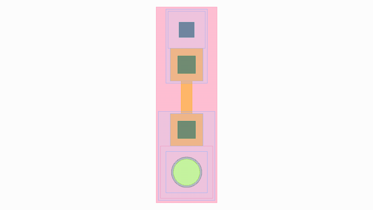
The figure below shows the output of the yTron PCell if the class was constructed inheriting from
spira.PCell. The metal layers are separated and the connection ports are still visible.
The following figure is the final result when inheriting from spira.Circuit
rather than spira.PCell. The contacting metal layers are merged and the redundant ports are filtered.
From the code above we can see that three routes are defined.
The first, connects the left arm with the first port using a basic manhattan structure.
The second and third, connects the right arm to the second port and the source arm to the third port,
but uses a sine path type to generate the routing polygons.
Via Device
Via devices generally following the same design patterns, but still require explicit construction
to describe how PDK data should be handled on instance creation. This example illustrated the
creation of the alternative resistor via contact that is responsible to connecting resistive
layer R5 to inductive layer M6.
Demonstrates
- How to create a via device.
- How to add range restrictions to parameters.
- How to create a cell that validates design rules on instance creation.
Recall, that by definition a PCell script is responsible for describing the interrelations between layout elements and defined parameters. These parameters can be design restrictions imposed by the specific fabrication technology.
class ViaC5RA(spira.Device):
    """ Via component for the MiTLL process. """

    width = spira.NumberParameter(default=RDD.R5.MIN_SIZE, restriction=spira.RestrictRange(lower=RDD.R5.MIN_SIZE))

    height = spira.Parameter(fdef_name='create_height')
    via_width = spira.Parameter(fdef_name='create_via_width')
    via_height = spira.Parameter(fdef_name='create_via_height')

    m6_width = spira.Parameter(fdef_name='create_m6_width', doc='Width of the via layer polygon.')
    m6_height = spira.Parameter(fdef_name='create_m6_height', doc='Width of the via layer polygon.')

    def create_m6_width(self):
        return (self.via_width + 2*RDD.C5R.M6_MIN_SURROUND)

    def create_via_width(self):
        return (self.width + 2*RDD.C5R.R5_MAX_SIDE_SURROUND)

    def create_via_height(self):
        return RDD.C5R.MIN_SIZE

    def create_height(self):
        return self.via_height + 2*RDD.R5.C5R_MIN_SURROUND

    def create_elements(self, elems):
        elems += spira.Box(layer=RDD.PLAYER.C5R.VIA, width=self.via_width, height=self.via_height, enable_edges=False)
        elems += spira.Box(alias='M6', layer=RDD.PLAYER.M6.METAL, width=self.m6_width, height=self.height, enable_edges=False)
        elems += spira.Box(alias='R5', layer=RDD.PLAYER.R5.METAL, width=self.width, height=self.height, enable_edges=False)
        return elems

    def create_ports(self, ports):
        p0 = self.elements['M6'].ports.unlock
        p1 = self.elements['R5'].ports.unlock
        return ports
Thus, the code for the via PCell defined above is responsible for describing how the top and bottom metal layers must be constructed in relation to the contact layer without violating any design rules. The PCell defines the specific design rules applicable to the creation of this via device.
Resistor
In Single Flux Quantum (SFQ) logic circuits, we typically use a shunt resistance for the biasing section of the circuit. Therefore, we would want to create a single resistor PCell that can be used as a template in more complex circuit PCells. Here, we design a resistor that parameterized its width, length, and type of via connection to other metal layers.
Demonstrates
- How to design a circuit that can interchange different via devices.
- How to restrict the circuit to only accept vias of a certain type.
- How to activate specific port edges that can be used for external connetions.
This PCell can iterate between two different vias connections that connect metal layer R5 and M6;
the alternative version of the standard version.
class Resistor(spira.Circuit):
    """ Resistor PCell of type Circuit between two vias connecting to layer M6. """

    length = spira.NumberParameter(default=7)
    width = spira.NumberParameter(
        default=RDD.R5.MIN_SIZE,
        restriction=spira.RestrictRange(lower=RDD.R5.MIN_SIZE),
        doc='Width of the shunt resistance.')
    via = spira.CellParameter(
        default=dev.ViaC5RS,
        restriction=spira.RestrictType([dev.ViaC5RA, dev.ViaC5RS]),
        doc='Via component for connecting R5 to M6')
    text_type = spira.NumberParameter(default=92)

    via_left = spira.Parameter(fdef_name='create_via_left')
    via_right = spira.Parameter(fdef_name='create_via_right')

    def validate_parameters(self):
        if self.length < self.width:
            raise ValueError('Length cannot be less than width.')
        return True

    def create_via_left(self):
        via = self.via(width=0.3+self.width)
        T = spira.Rotation(rotation=-90)
        S = spira.SRef(via, transformation=T)
        return S

    def create_via_right(self):
        via = self.via(width=0.3+self.width)
        T = spira.Rotation(rotation=-90, rotation_center=(self.length, 0))
        S = spira.SRef(via, midpoint=(self.length, 0), transformation=T)
        return S

    def create_elements(self, elems):

        elems += [self.via_left, self.via_right]

        elems += RouteStraight(
            p1=self.via_left.ports['E0_R5'],
            p2=self.via_right.ports['E2_R5'],
            layer=RDD.PLAYER.R5.METAL)

        return elems

    def create_ports(self, ports):

        ports += self.via_left.ports['E1_M6'].copy(name='P1_M6')
        ports += self.via_left.ports['E2_M6'].copy(name='P2_M6')
        ports += self.via_left.ports['E3_M6'].copy(name='P3_M6')

        ports += self.via_right.ports['E0_M6'].copy(name='P4_M6')
        ports += self.via_right.ports['E1_M6'].copy(name='P5_M6')
        ports += self.via_right.ports['E3_M6'].copy(name='P6_M6')

        return ports
The length parameter can be any value as long as it is larger than the width. Therefore, the
length parameter has no restrictions, but are validated once all parameters have been defined using the
validate_parameters method. The width parameter is restricted to a minimum size,
which implicitly mean the length is also restricted to this size value. The via parameter
has to be a PCell class and has to be of type dev.ViaC5RA or dev.ViaC5RS.
We only want to connect to the connection vias of the instance, and therefore we only activate the ports
of the two via instance, instead of activating all possible edge ports, as shown in the create_ports method.
Josephson Junction
The Josephson junction is the most important device in any SDE circuit. We want to create a junction PCell that parameterizes the following device attributes:
- The shunt resistor width.
- The shunt resistor length.
- The junction layer radius.
- Boolean parameters to include/exclude via connections to ground and skyplane.
Demonstrates
- How to design a fully parameterized Josephson junction.
- How to add a bounding box around a set of polygon objects.
The design of the junction is broken down into three sections; a top section, a bottom section, and the shunt
resistor that connects the top and bottom sections. The top and bottom section each are wrapped with a
bounding box polygon of metal layer M6.
class __Junction__(spira.Cell):
    """ Base class for Junction PCell. """

    radius = spira.NumberParameter()
    width = spira.NumberParameter(doc='Shunt resistance width')
    c5r = spira.Parameter(fdef_name='create_c5r')


class I5Contacts(__Junction__):
    """ Cell that contains all the vias of the bottom halve of the Junction. """

    i5 = spira.Parameter(fdef_name='create_i5')
    i6 = spira.Parameter(fdef_name='create_i6')

    sky_via = spira.BoolParameter(default=False)

    def create_i5(self):
        via = dev.ViaI5()
        V = spira.SRef(via, midpoint=(0,0))
        return V

    def create_i6(self):
        c = self.i5.midpoint
        w = (self.i5.ref.width + 4*RDD.I6.I5_MIN_SURROUND)
        via = dev.ViaI6(width=w, height=w)
        V = spira.SRef(via, midpoint=c)
        return V

    def create_c5r(self):
        # via = dev.ViaC5RA(width=self.width)
        via = dev.ViaC5RS()
        V = spira.SRef(via)
        if self.sky_via is True:
            V.connect(port=V.ports['E0_R5'], destination=self.i6.ports['E2_M6'], ignore_process=True)
        else:
            V.connect(port=V.ports['E0_R5'], destination=self.i5.ports['E2_M5'], ignore_process=True)
        return V

    def create_elements(self, elems):

        # Add the two via instances.
        elems += [self.i5, self.c5r]

        # Add the skyplane via instance if required.
        if self.sky_via is True:
            elems += self.i6

        # Add bounding box around all elements.
        box_shape = elems.bbox_info.bounding_box(margin=0.1)
        elems += spira.Polygon(shape=box_shape, layer=RDD.PLAYER.M6.METAL)

        return elems

    def create_ports(self, ports):
        ports += self.i5.ports['E2_M5'].copy(name='P2_M5')
        ports += self.c5r.ports['E2_R5'].copy(name='P2_R5')
        return ports


class J5Contacts(__Junction__):
    """ Cell that contains all the vias of the top halve of the Junction. """

    j5 = spira.Parameter(fdef_name='create_j5')

    def create_j5(self):
        jj = dev.JJ(width=2*self.radius)
        D = spira.SRef(jj, midpoint=(0,0))
        return D

    def create_c5r(self):
        # via = dev.ViaC5RA(width=self.width)
        via = dev.ViaC5RS()
        V = spira.SRef(via)
        V.connect(port=V.ports['E0_R5'], destination=self.j5.ports['E0_M5'], ignore_process=True)
        return V

    def create_elements(self, elems):

        # Add the two via instances.
        elems += [self.j5, self.c5r]

        # Add bounding box around all elements.
        box_shape = elems.bbox_info.bounding_box(margin=0.1)
        elems += spira.Polygon(shape=box_shape, layer=RDD.PLAYER.M6.METAL)

        return elems

    def create_ports(self, ports):
        ports += self.j5.ports['E0_M5'].copy(name='P0_M5')
        ports += self.c5r.ports['E2_R5'].copy(name='P2_R5')
        return ports
The J5Contacts and I5Contacts classes are the top and bottom sections, respectively.
The __Junction__ class is a base class that contains parameters common to both of these classes.
As shown in the create_elements methods for both classes a metal bounding box is added around
all defined elements.
The results for J5Contacts is shown below and consists of a C5R via that connects
layer R5 and a junction via that contains the actually junction layer.
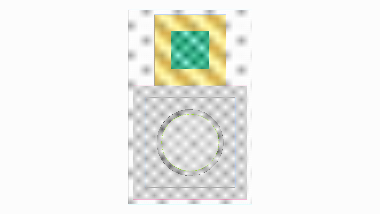
The result for I5Contacts is shown below and consists of a C5R via that connects
layer R5 and a I5 via that connects layer M5 to layer M6. The skyplane via that connects
M6 to M7 is optional depending on the boolean value of the sky_via parameter.
class Junction(spira.Device):

    text_type = spira.NumberParameter(default=91)

    length = spira.NumberParameter(default=1.5, doc='Length of the shunt resistance.')

    width = spira.NumberParameter(
        default=RDD.R5.MIN_SIZE,
        restriction=spira.RestrictRange(lower=RDD.R5.MIN_SIZE, upper=RDD.R5.MAX_WIDTH),
        doc='Width of the shunt resistance.')

    radius = spira.NumberParameter(
        default=RDD.J5.MIN_SIZE,
        restriction=spira.RestrictRange(lower=RDD.J5.MIN_SIZE, upper=RDD.J5.MAX_SIZE),
        doc='Radius of the circular junction layer.')

    i5 = spira.Parameter(fdef_name='create_i5_cell')
    j5 = spira.Parameter(fdef_name='create_j5_cell')

    gnd_via = spira.BoolParameter(default=False)
    sky_via = spira.BoolParameter(default=False)

    def create_i5_cell(self):
        D = I5Contacts(width=self.width, radius=self.radius, sky_via=self.sky_via)
        S = spira.SRef(D)
        S.move(midpoint=S.ports['P2_R5'], destination=(0, self.length))
        return S

    def create_j5_cell(self):
        D = J5Contacts(width=self.width, radius=self.radius)
        S = spira.SRef(D)
        S.move(midpoint=S.ports['P2_R5'], destination=(0,0))
        return S

    def create_elements(self, elems):

        elems += self.i5
        elems += self.j5

        elems += RouteStraight(
            p1=self.i5.ports['P2_R5'].copy(width=self.width),
            p2=self.j5.ports['P2_R5'].copy(width=self.width),
            layer=RDD.PLAYER.R5.METAL)

        if self.gnd_via is True:
            i4 = dev.ViaI4()
            elems += spira.SRef(i4, midpoint=m5_block.center)

        box_shape = elems.bbox_info.bounding_box(margin=0.1)
        elems += spira.Polygon(shape=box_shape, layer=RDD.PLAYER.M5.METAL)

        return elems

    def create_ports(self, ports):
        ports += self.j5.ports['E0_M6'].copy(name='P0_M6')
        ports += self.j5.ports['E1_M6'].copy(name='P1_M6')
        ports += self.j5.ports['E3_M6'].copy(name='P3_M6')
        ports += self.i5.ports['E1_M6'].copy(name='P4_M6')
        ports += self.i5.ports['E2_M6'].copy(name='P5_M6')
        ports += self.i5.ports['E3_M6'].copy(name='P6_M6')
        return ports
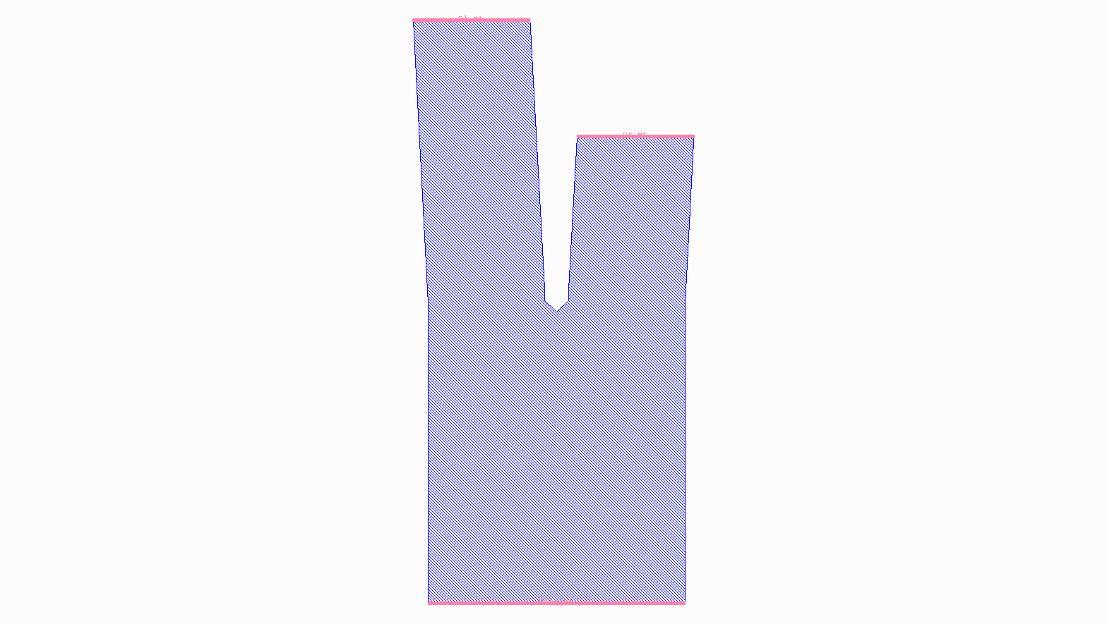
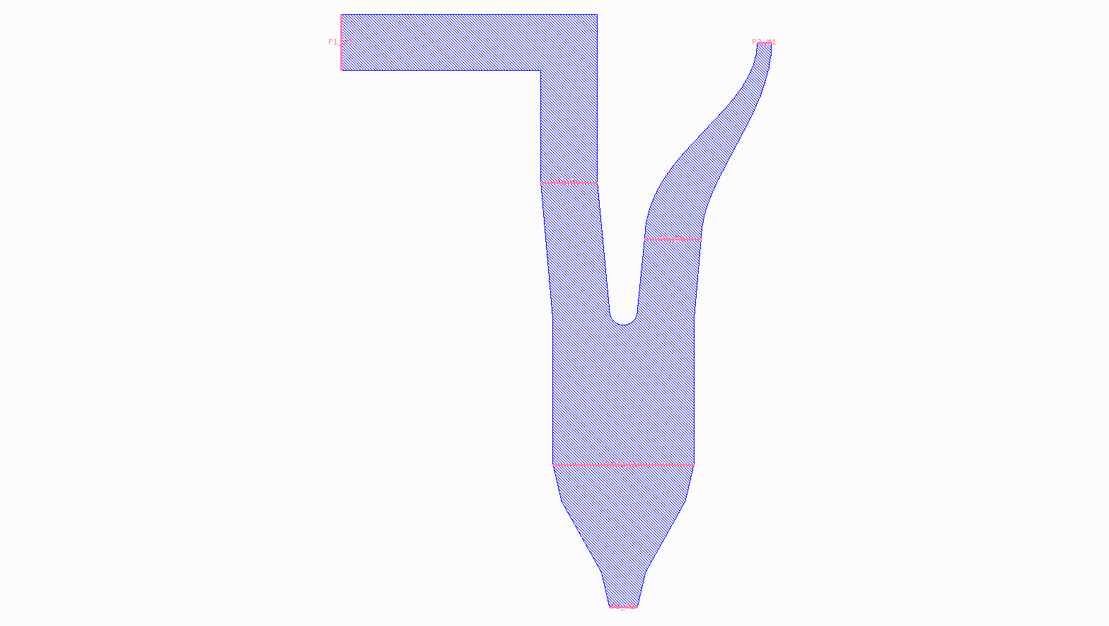
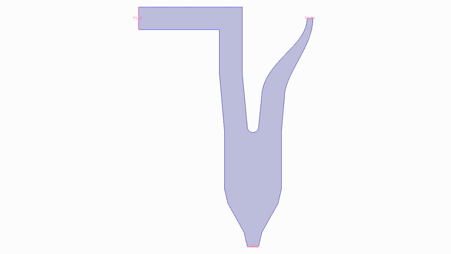
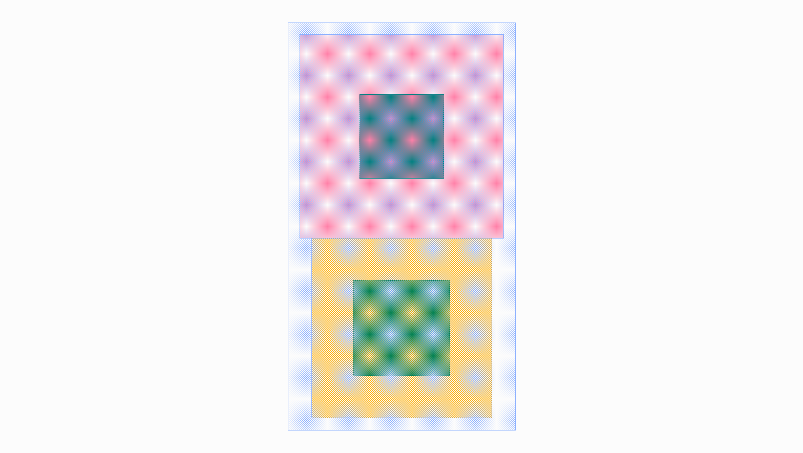
The Junction class is created and instances of the J5Contacts and I5Contacts
cells are added and moved relative to eachother with a separation distance equal to the length of the shunt resistor.
The instances of of these two cells are then connection via a resistive route. For debugging purposes we can disable
the operations preformed by the spira.Device class by setting pcell=False. The output is shown below
displays the individual layers of each instance.
By enabling PCell operations again we can see that the overlapping metal layers are merged by similar process polygon, as shown in the figure below.
Josephson Transmission Line
The Josephson Transmission Line (JTL) is the most basic SFQ circuit and consist of two junctions, an input and output port, and a biasing port.
Demonstrates
- How to define routes between different ports and devices.
- How to parameterize the route widths.
- How to include a device PCell into higher hierarchical designs.
We define three width parameters to control the polygon routing width between:
- The input port and first junction.
- The ouput port and second junction.
- The first junction and second junction.
Next, we create a set of create methods to define device and port instances.
class Jtl(spira.PCell):

    w1 = spira.NumberParameter(
        default=RDD.M6.MIN_SIZE,
        restriction=RestrictRange(lower=RDD.M6.MIN_SIZE, upper=RDD.M6.MAX_WIDTH),
        doc='Width of left inductor.'
    )
    w2 = spira.NumberParameter(
        default=RDD.M6.MIN_SIZE,
        restriction=RestrictRange(lower=RDD.M6.MIN_SIZE, upper=RDD.M6.MAX_WIDTH),
        doc='Width of middle inductor.'
    )
    w3 = spira.NumberParameter(
        default=RDD.M6.MIN_SIZE,
        restriction=RestrictRange(lower=RDD.M6.MIN_SIZE, upper=RDD.M6.MAX_WIDTH),
        doc='Width of rigth inductor.'
    )

    p1 = spira.Parameter(fdef_name='create_p1')
    p2 = spira.Parameter(fdef_name='create_p2')
    p3 = spira.Parameter(fdef_name='create_p3')
    p4 = spira.Parameter(fdef_name='create_p4')

    jj1 = spira.Parameter(fdef_name='create_jj_left')
    jj2 = spira.Parameter(fdef_name='create_jj_right')

    shunt = spira.Parameter(fdef_name='create_shunt')

    bias_res = spira.Parameter(fdef_name='create_bias_res')
    via1 = spira.Parameter(fdef_name='create_via1')

    def create_p1(self):
        p1 = spira.Port(name='P1_M6', width=self.w1)
        return p1.distance_alignment(port=p1, destination=self.jj1.ports['P1_M6'], distance=-10)

    def create_p2(self):
        p2 = spira.Port(name='P2_M6', width=self.w1)
        return p2.distance_alignment(port=p2, destination=self.jj2.ports['P3_M6'], distance=10)

    def create_p3(self):
        return spira.Port(name='P3_M6', midpoint=(0, 15), orientation=270, width=self.w1)

    def create_p4(self):
        return spira.Port(name='P4_M6', midpoint=(0, 1.5), orientation=90, width=self.w1)

    def create_jj_left(self):
        jj = dev.Junction(length=1.9, width=1, radius=0.91)
        T = spira.Rotation(rotation=180, rotation_center=(-10,0))
        S = spira.SRef(jj, midpoint=(-10,0), transformation=T)
        return S

    def create_jj_right(self):
        jj = dev.Junction(length=1.9, width=1, radius=0.91)
        T = spira.Rotation(rotation=180, rotation_center=(10,0))
        S = spira.SRef(jj, midpoint=(10,0), transformation=T)
        return S

    def create_shunt(self):
        D = Resistor(width=1, length=3.7)
        S = spira.SRef(reference=D, midpoint=(0,0))
        S.distance_alignment(port='P2_M6', destination=self.p3, distance=-2.5)
        return S

    def create_elements(self, elems):

        elems += self.jj1
        elems += self.jj2
        elems += self.shunt

        elems += RouteStraight(p1=self.p1,
            p2=self.jj1.ports['P1_M6'].copy(width=self.p1.width),
            layer=RDD.PLAYER.M6.ROUTE)

        elems += RouteStraight(p1=self.p2,
            p2=self.jj2.ports['P3_M6'].copy(width=self.p2.width),
            layer=RDD.PLAYER.M6.ROUTE)

        elems += RouteStraight(
            p1=self.jj1.ports['P3_M6'].copy(width=self.w2),
            p2=self.jj2.ports['P1_M6'].copy(width=self.w2),
            layer=RDD.PLAYER.M6.ROUTE)

        elems += RouteStraight(p1=self.shunt.ports['P2_M6'], p2=self.p3, layer=RDD.PLAYER.M6.ROUTE)
        elems += RouteStraight(p1=self.shunt.ports['P4_M6'], p2=self.p4, layer=RDD.PLAYER.M6.ROUTE)

        return elems

    def create_ports(self, ports):
        ports += self.p1
        ports += self.p2
        ports += self.p3
        ports += self.p4
        return ports
This examples place two junctions, jj_left and jj_right, at positions (-10,0) and
(10,0). The input port is placed a ditance of -10 to the left of jj_left, and the ouput port
a distance of 10 to the right of jj_right.
The biasing port, p3 is place at position (0,15) and port P2_M6 of the biasing resistor PCell
is place a distance of 2.5 to the bottom of p3.
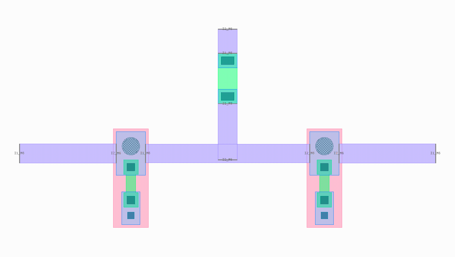
Electrical Rule Checking
The electrical rule checking algorithm is applied on an instance using a filtering method. Therefore, it is easily enabled/disabled for debugging purposes.
Demonstrates
- How to toggle the ERC algorithm.
- How to view the electrical rule checking results using virtual modeling.
# Create an instance of the PCell class.
D = Jtl()

# Apply the ERC and Port Excitation algorithms to the cell.
f = RDD.FILTERS.PCELL.MASK

D = f(D)

from spira.yevon.vmodel.virtual import virtual_connect
v_model = virtual_connect(device=D)

v_model.view_virtual_connect(show_layers=True)
The resultant layout or view of a cicuit that contains virtual elements that will not be included in the final design, is called a virtual model. The above example illustrates how electrical rule checking can be debugged using virtually constructed polygons.
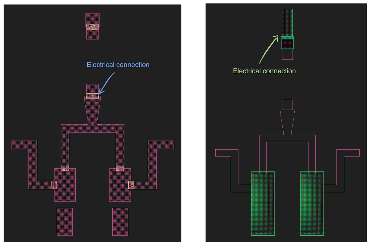
Netlist Extraction
Netlists for PCells can be extracted and viewed in a graph representation.
Demonstrates
- How to extract the netlist graph of a PCell.
- How to view the extracted graph.
# Create an instance of the PCell class.
D = Jtl()

# Apply the ERC and Port Excitation algorithms to the cell.
D = RDD.FILTERS.PCELL.MASK(D)

# Extract the physical netlist.
net = D.extract_netlist

# View the netlist.
D.netlist_view(net=net)
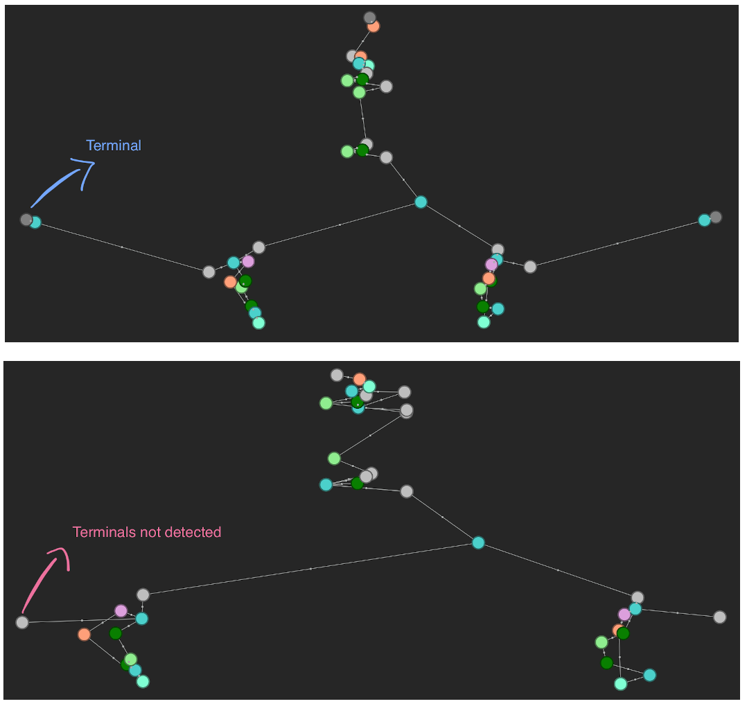
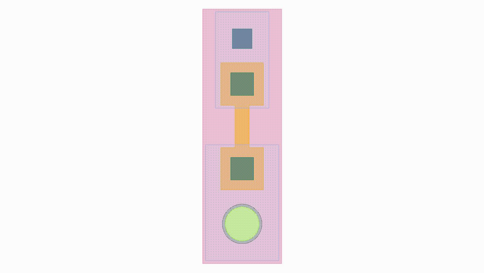
Before running the netlist extraction algorithm it is important to first apply the required filters to the pcell instance. These filters includes running electrical rule checking algorithm and compressing terminal ports down onto their corresponding polygon instances. It is also possible to toggle certain filters for debugging purposes:
D = Jtl()

f = RDD.FILTERS.PCELL.MASK

f['pin_attach'] = False

D = f(D)

net = D.extract_netlist

D.netlist_view(net=net)
The above example illustrates the extracted netlist if the pin attach algorithm is disabled. The added terminal ports are not detected by the netlist run, since they are not compressed down the layout hierarchy onto their corresponding polygons. The following image shows the different extracted netlists for a basic JTL layout using the code snippets previously discussed.